Spark Plasma Sintering “SPS” (aka FAST or Field Assisted Sintering Technology) is an advanced technique to take powder and turn it into solid parts similar to additive manufacturing but without having to melt the material. It allows for the rapid application of temperature and pressure via high-density pulsed current within a controlled atmosphere. The unique heating mechanism of using electrical current gives SPS the ability to consolidate materials that traditional processes can’t and at much faster rates. SPS is the ideal consolidation and bonding method for all of your materials including metals, refractory alloys, nanomaterials, ultra-high temp ceramics, and more. In simple terms, SPS can be thought of as a way of making strong and dense materials from powders using high heat and pressure.
Click here to listen to the latest episode of the Materialism podcast which features our CEO Eric Eyerman talking about Spark Plasma Sintering!
Overall Benefits of SPS
- Shorter Cycle Times - Sintering cycles are minutes vs hours/days for conventional processes. High productivity, extremely rapid material development capabilities.
- Lower Sintering Temperatures - Sinter materials at lower temperatures compared to conventional sintering processes
- Extremely Versatile - Densify low melting point metals, ultra-high temperature ceramics, or even bond dissimilar materials requiring nonuniform temperature. No other sintering process can come close. Can sinter porous parts and fully dense parts.
- High-precision process control - Able to finely control sintering parameters including temperature and pressure to ensure the best outcome for your parts. Unique chemistries are unable to be made with conventional liquid melt processes. Engineered structures within materials preserved that would otherwise be lost in other processes
SPS & Powder Metallurgy:
Spark plasma sintering (SPS) is a cutting-edge technique within the powder metallurgy industry, revolutionizing the fabrication of advanced materials. It involves applying high electrical current and pressure to compact powder particles, resulting in rapid consolidation and sintering. This process enables the production of high-density components with fine microstructures and enhanced mechanical properties, making it invaluable for manufacturing applications in aerospace, automotive, electronics, and healthcare sectors. By significantly reducing processing time and energy consumption while maintaining superior quality, SPS contributes to the advancement of powder metallurgy as a versatile and efficient manufacturing method, meeting the increasing demand for high-performance materials in various industries.
Just a few applications of SPS
- Energy Storage: High-capacity lithium-ion batteries and other advanced energy storage materials
- Biomedical Engineering: Porous ceramics for drug delivery and scaffolds for tissue engineering
- Advanced Ceramics: High-temperature superconductors and high-performance piezoelectric ceramics
- Intermetallics: Advanced alloys with improved mechanical, thermal, and electrical properties
- Composites: Reinforced ceramics and metals with enhanced mechanical properties
Diffusion Bonding using SPS
Not only can SPS densify powder materials but it is also highly effective at bonding both similar and dissimilar materials together. Bonding can be performed with all the materials listed above and more. Options for bonding include:
- Bulk solid to bulk solid materials
- Powder to solid
- Bonding thin sheets together
- Functionally graded material bonding (ceramics to metals, polymers to metals, etc.)
Additional resources to learn about SPS/FAST:
Fast-SPS Booklet 2023
https://onlinelibrary.wiley.com/doi/full/10.1002/adem.201300409
https://www.sciencedirect.com/topics/engineering/spark-plasma-sintering
https://www.totalmateria.com/page.aspx?ID=CheckArticle&site=kts&NM=460
| Classification |
Materials for SPS processing |
|
| Metals |
Virtually any metals possible: Fe, Cu, Al, Au, Ag, Ni, Cr, Mo, Sn, Ti, W, Be |
|
| Ceramics |
Oxides
Carbides
Nitrides
Borides
Flourides |
Al2O3, Mulite, ZrO2, MgO, SiO2, TiO2, HfO2
SiC, B4C, TaC, TiC, WC, ZrC, VC
Si3N4, TaN, TiN, AiN, ZrN, VN
TiB2, HfB2, LaB6, ZrB2, VB2
LiF, CaF2, MgF2 |
| Cermets |
Si3N4+Ni, Al2O3+Ni, ZrO2+Ni
Al2O3+TiC, SUS+ZrO2, Al2O3+SUS
SUS+WC/Co, BN+Fe. WC+Co+Fe |
|
| Intermetalic compounds |
TiAl. MoSi2, Si3Zr5,NiAl
NbCo, NbAl, LaBaCuSO4, Sm2Co17 |
|
| Other materials |
Organic materials (polyimide, etc.), compositematerials |
|
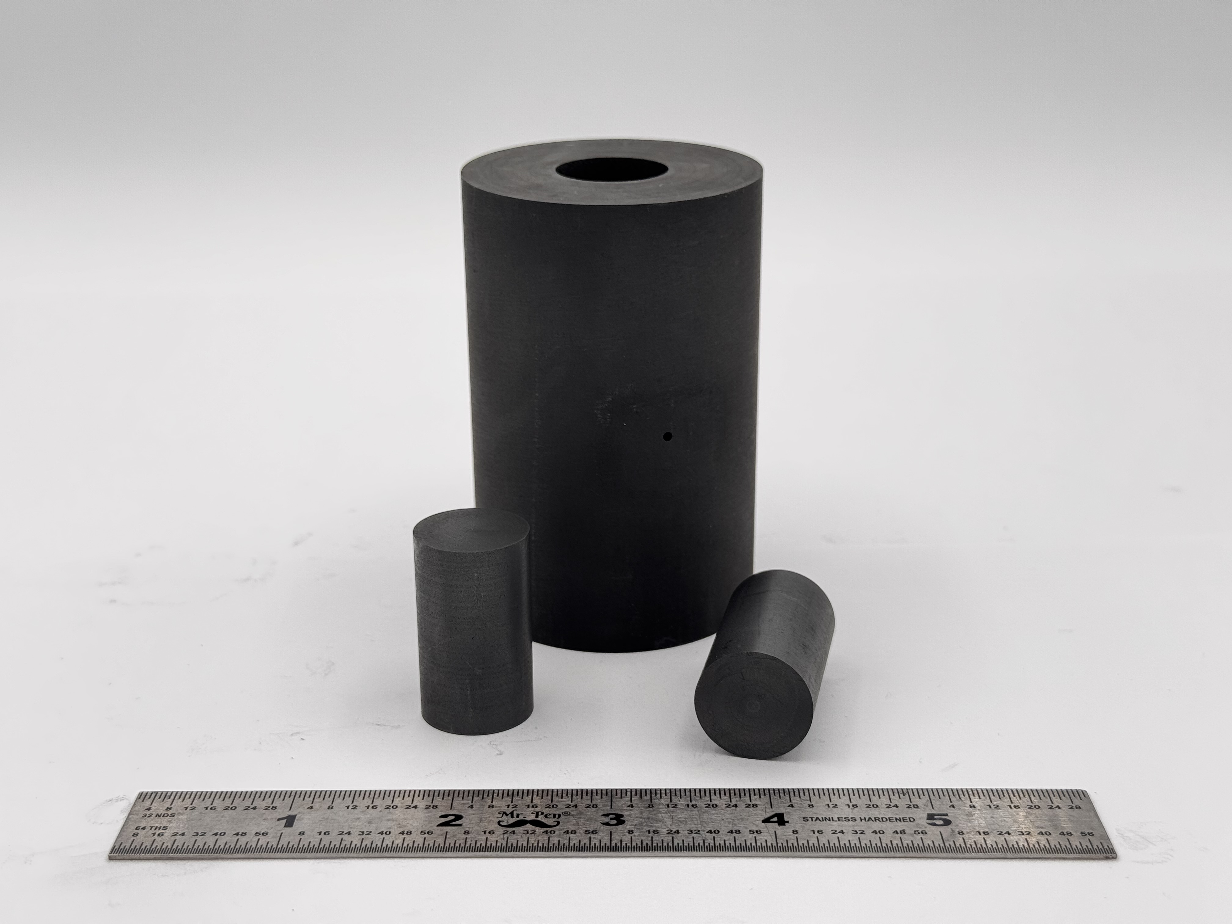 High Strength SPS Graphite Tooling
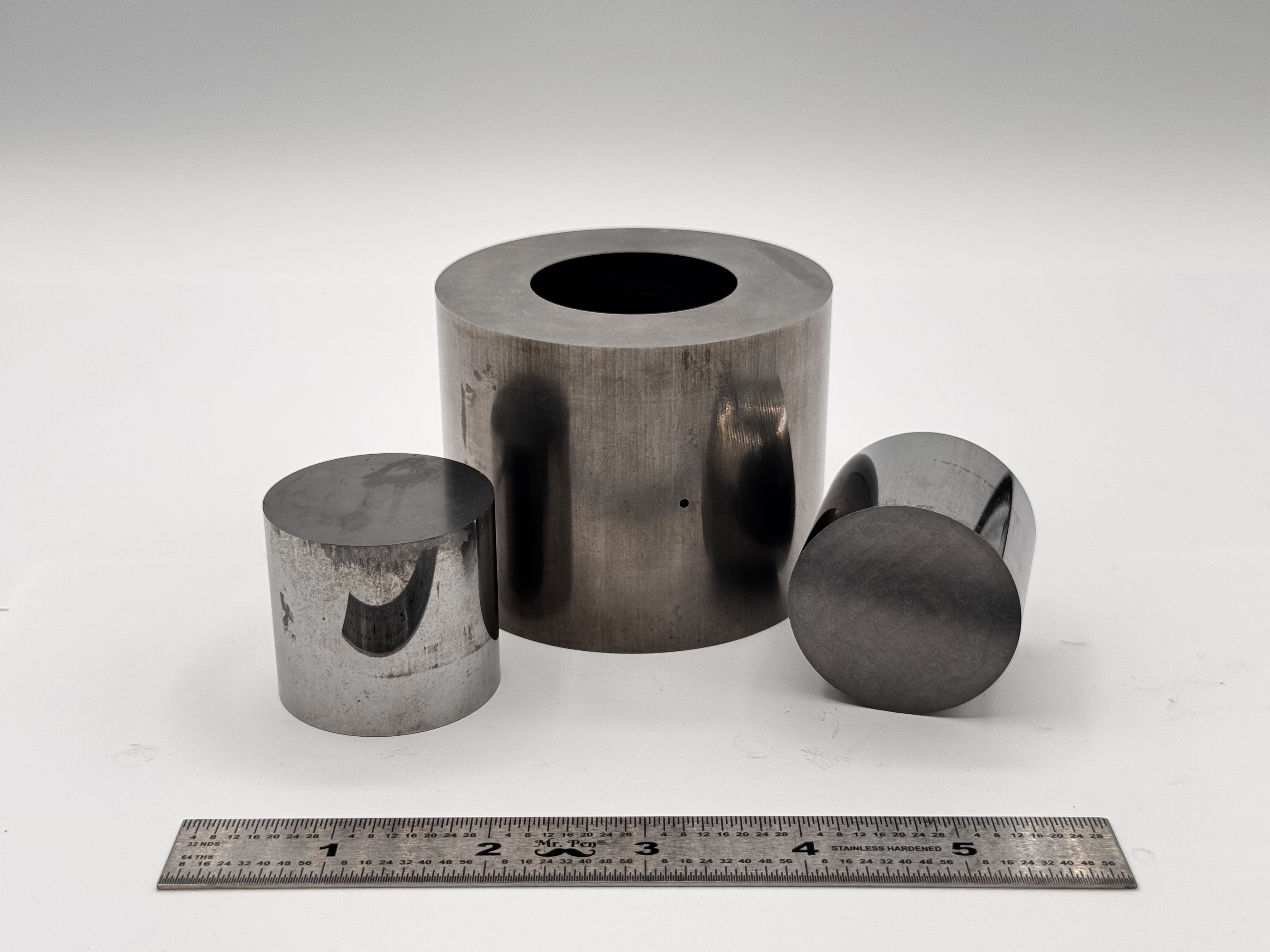 Tungsten Carbide Tooling
 Carbon Graphite Foil / Paper
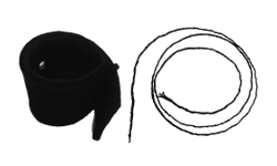 Carbon Felt and Yarn
 Spark Plasma Sintering Systems
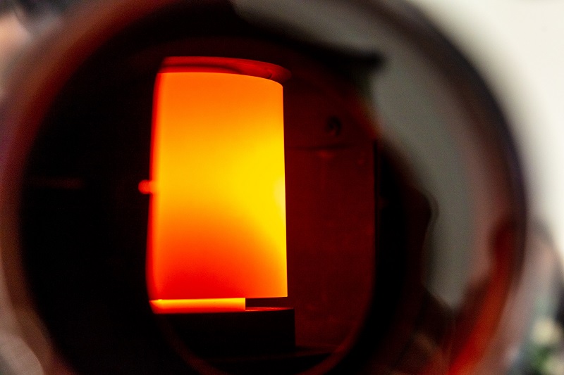 SPS/FAST Modeling Software