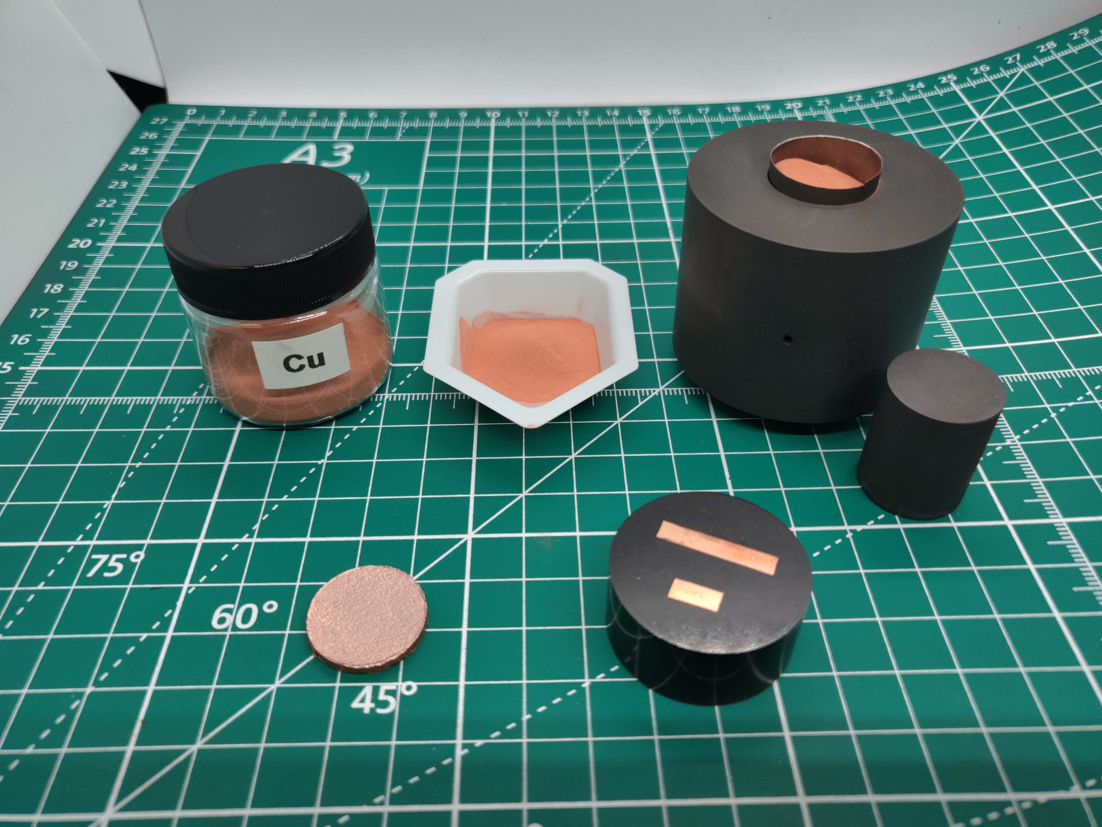
 SPS Starter Accessory Kits
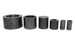
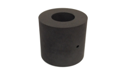
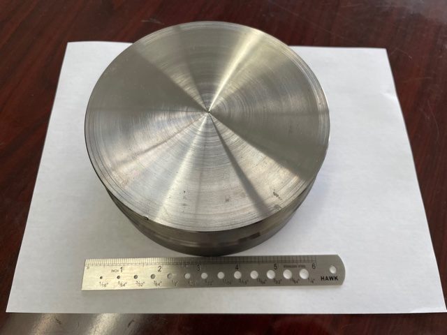
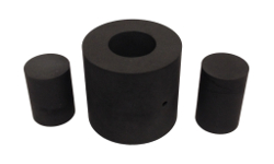 High Strength SPS Graphite Tooling
 Tungsten Carbide Tooling
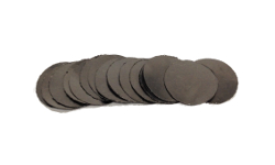
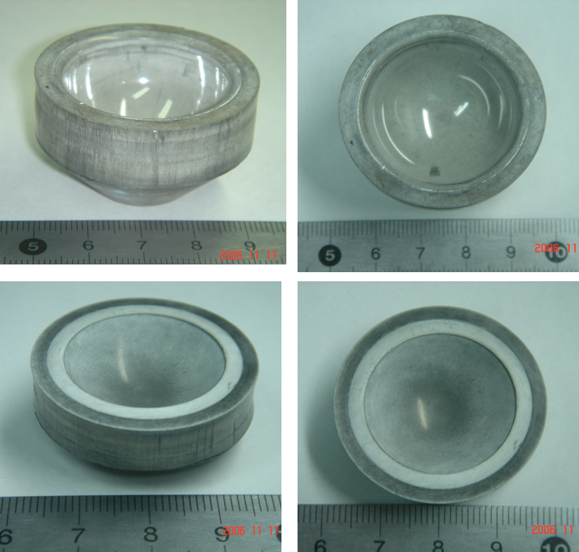
 SPS Graphite Crucibles
 Carbon Graphite Foil / Paper
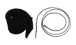 Carbon Felt and Yarn
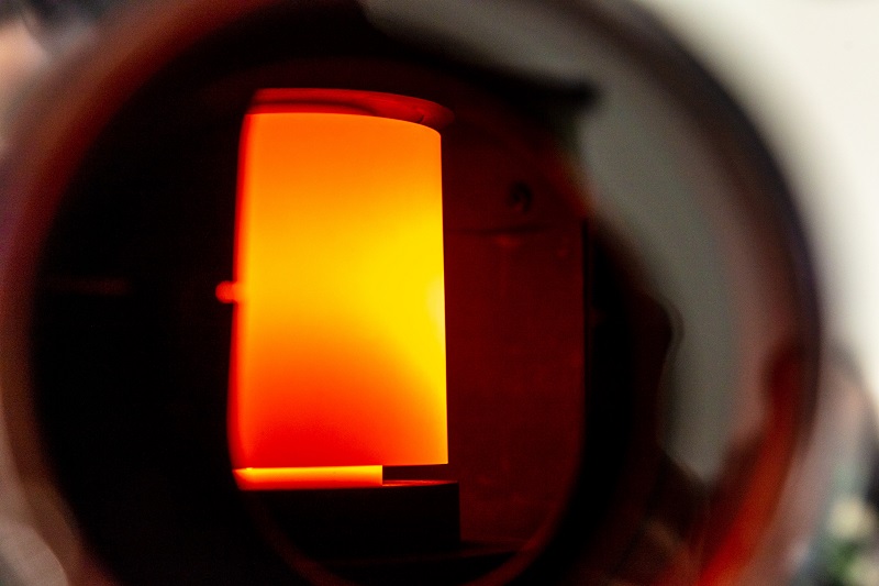
 Quartz Glass Windows
 SPS/FAST Modeling Software
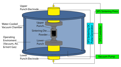
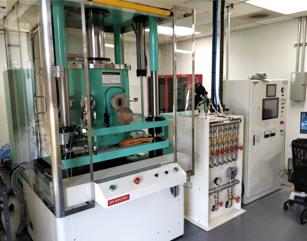
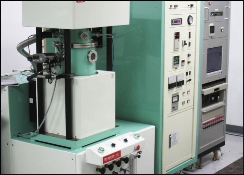
Spark Plasma / Field Assisted Sintering (SPS/FAST)
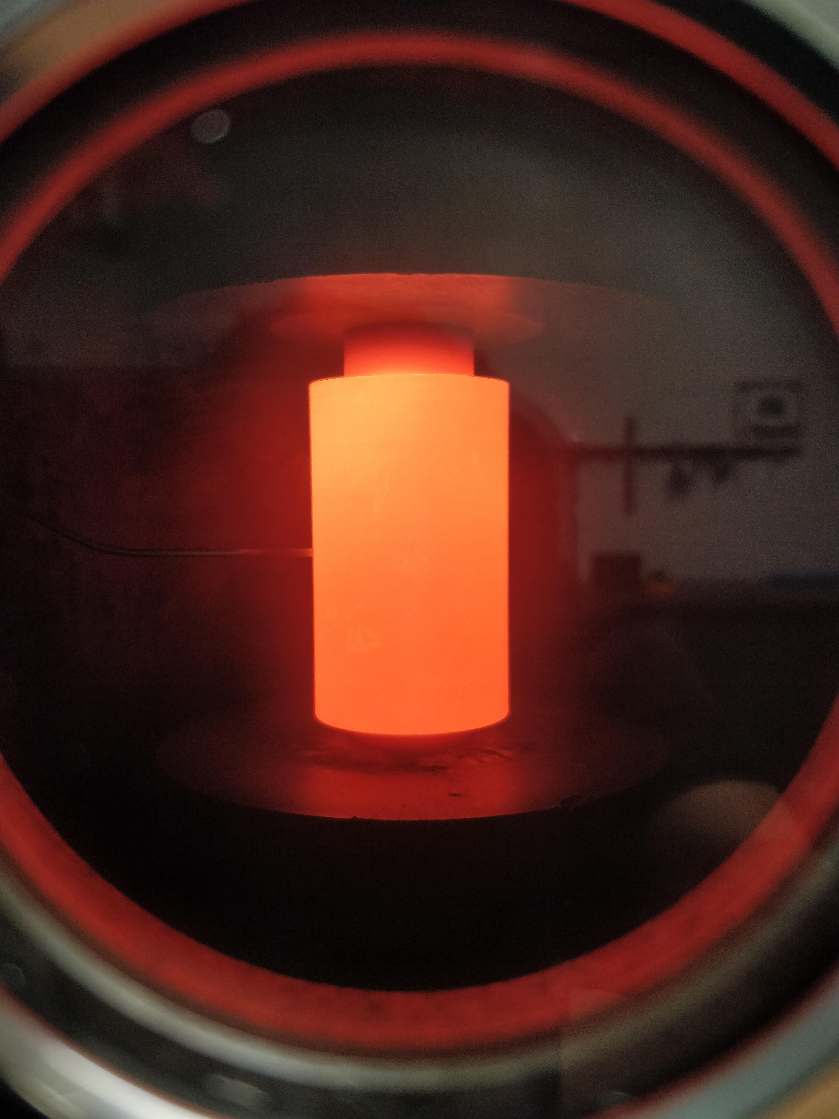
SPS (aka FAST or Field Assisted Sintering Technology) allows for the rapid application of temperature and pressure via high-density pulsed current within a controlled atmosphere. SPS is the ideal consolidation and bonding method for all of your materials including metals, refractory alloys, nanomaterials, ultra-high temp ceramics, and more.
The team here at Cal Nano has over a decade of SPS experience sintering tens of thousands of samples with a wide variety of materials.
Cal Nano SPS/FAST Toll Services:
- Collaborative R&D, prototyping and pilot-scale production services are available
- High-quality customer service & quick turnaround times
- Customers can provide powder or it can be sourced by Cal Nano
- Sintering available in sizes from ranging from 5 mm to 17" OD!
If interested in purchasing your own SPS equipment, please contact us for more information.
Spark Plasma Sintering Podcast
California Nanotechnologies - Intro to Spark Plasma Sintering
Cal Nano offers an array of unique capabilities for sintering or bonding your materials.
- Sinter or bond your materials in minutes while minimizing grain growth and retaining complex microstructure
- Most powders can be densified to 99%+
- Rapid iteration testing of your materials - cycles can be completed in as a few minutes
- Multiple inert atmosphere glove boxes for safe and effective powder handling
- Controlled densification to create porous samples is also possible
- Bonding of similar and dissimilar materials
- Near net-shape sintering
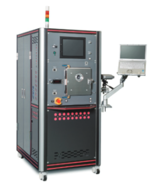
R&D Lab Scale SPS system
- Max Temperature - 2500 C
- Max Force - 50 kN (5 ton)
- Max Amperage - 1,500 Amps
- Max sample size - 1" OD x 1" tall (depending on temperature required)
- Automated chamber & vacuum systems
- Inert & forming gas atmosphere capability
- Manual & automatic cycles
Pilot Scale SPS system
- Max Temperature - 2500 C
- Max Force - 1000 kN (100 ton)
- Max Amperage - 10,000 Amps
- Max sample size - 6" OD x 4" tall (depending on temperature required)
- Automated chamber & vacuum systems
- Inert & forming gas atmosphere capability
- Manual & automatic cycles
Production Scale SPS system
- Max Temperature - 2500 C
- Max Force - 5000 kN (500 ton)
- Max Amperage - 85,000 Amps
- Max sample size - 17" OD x 6" tall (depending on temperature required)
- Automated chamber & vacuum systems
- Inert & forming gas atmosphere capability
- Manual & automatic cycles
Field Assisted Sintering can be used to consolidate nearly any powdered material you can think of. Here are some but not all of the materials/applications:
- Batteries - soft & permanent magnets (Nd, FeN, etc.. material)
- Semiconductors
- Fine Ceramics
- Thermoelectrics
- Functionally Graded Materials
- Electronics
- Nanophases
- Hard Alloy Tools
- Diamond Tools
- Biomaterials
- Porous Materials
- Molds and Dies
These are all referencing the same technology so there is no difference. SPS (Spark Plasma Sintering) was the original name of the technology and is seen the most in academic literature. FAST (Field Assisted SIntering Technique) and PECS (Pulsed Electric Current Sintering) are used often by manufacturers and industry.
This has been a widely debated topic in the academic community but the short answer is no. No sparks or plasma has been observed during the process.
Yes! SPS/FAST is a great technology for both R&D and production. In the past, many in the industry have thought that it can only be used in the R&D lab but our work along with others in the field have proven that with the right applications, SPS can be used for mass production.
There are very few materials that you are not able to sinter with FAST/SPS. From low-temperature metals to ultra-high temperature ceramics and everything in between, SPS can consolidate most materials. This includes materials that are not electrically conductive.
Yes. Cal Nano is the North American Representative for the Japanese SPS equipment manufacturer SUGA. Before that we represented FUJI-SPS. Cal Nano has sold, installed, serviced and trained personnel on SPS equipment for nearly a decade.
Spark plasma sintering can produce materials with improved properties compared to traditional sintering methods, such as higher density, uniform structure, and improved strength. Additionally, SPS can be used to process materials that are difficult to sinter using traditional methods, such as nanoscale powders and high-temperature materials along with the ability to diffusion bond. SPS is faster, saves more energy, and is more cost-effective than other sintering techniques.
Spark plasma sintering is used in a wide range of industries, including aerospace, automotive, energy, and electronics. It is particularly useful for producing dense, strong materials for high-temperature applications and for processing materials that are difficult to sinter using traditional methods.
SPS Products & Accessories Catalog
CalNano's SPS (Spark Plasma Sintering) Product Catalog offers a comprehensive array of innovative materials and equipment to meet the diverse demands of research, manufacturing, and industrial applications. Their product lineup includes cutting-edge SPS systems, starter accessory kits for newcomers, and high-strength graphite and tungsten carbide tooling for precision shaping and efficient consolidation. Additionally, their high-quality graphite crucibles, carbon graphite foil, and insulation materials like carbon felt and yarn cater to various applications, while their transparent quartz glass windows find utility in high-temperature environments. To further enhance the SPS process, CalNano provides SPS/FAST modeling software for predictive control and optimization. These offerings underscore CalNano's commitment to delivering advanced solutions, designed to meet the needs of a wide range of industries, from aerospace to healthcare, with precision, quality, and innovation.