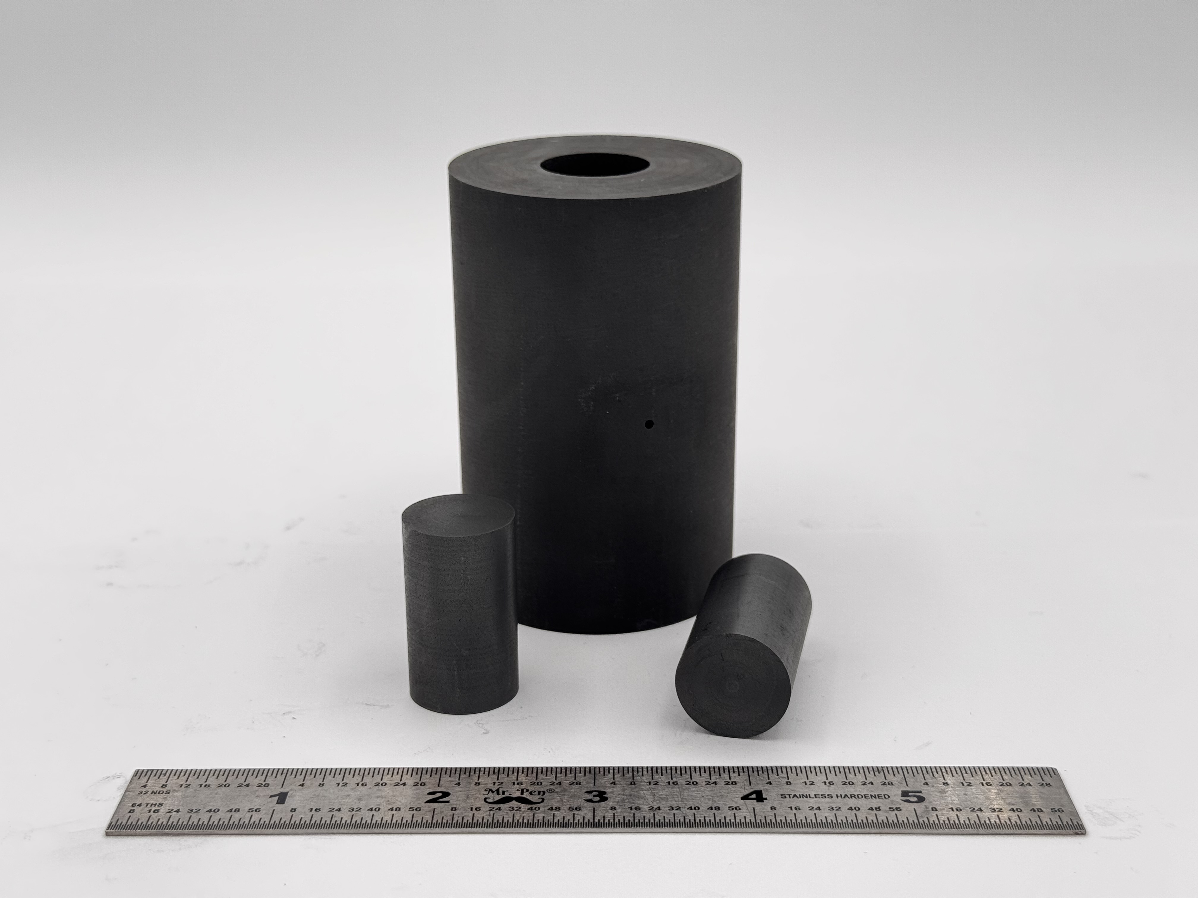
 High Strength SPS Graphite Tooling
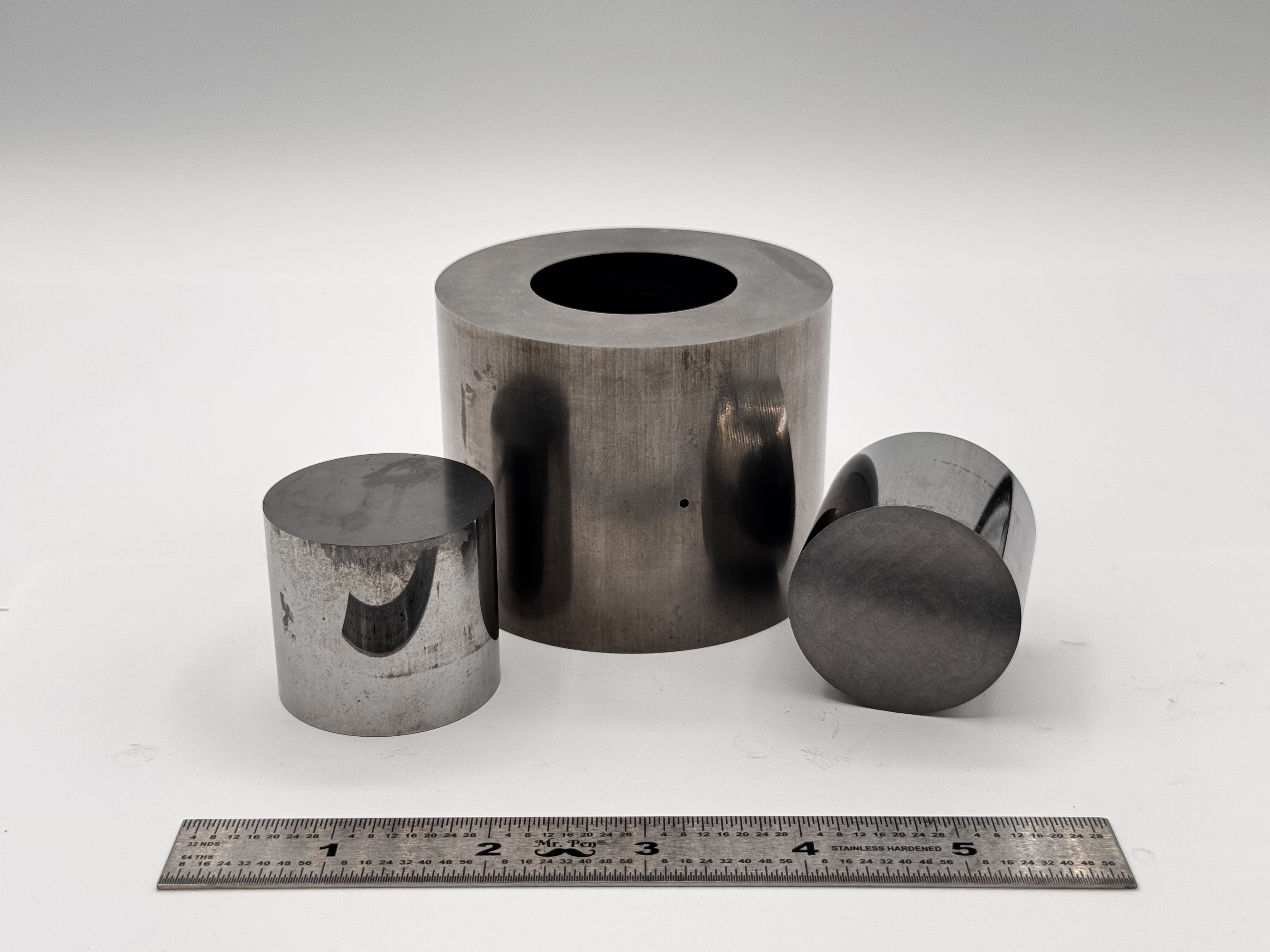 Tungsten Carbide Tooling
 Carbon Graphite Foil / Paper
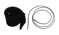 Carbon Felt and Yarn
 Spark Plasma Sintering Systems
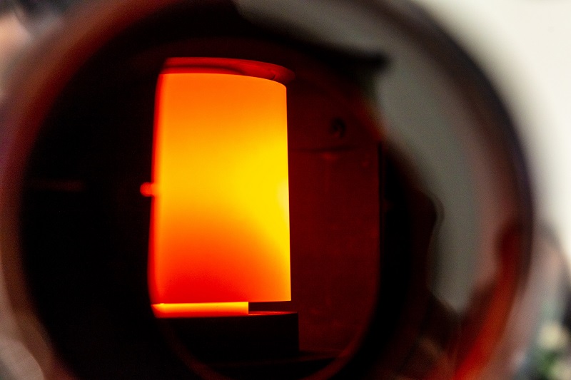 SPS/FAST Modeling Software
Transforming Materials Engineering with Spark Plasma Sintering Systems
In the realm of materials science and engineering, innovation is the key to unlocking the potential of new materials for a myriad of applications. At the forefront of this innovation stands Spark Plasma Sintering (SPS) technology, a revolutionary method for consolidating powders into dense, high-performance materials. California Nanotechnologies is proud to be a leading provider of Spark Plasma Sintering Systems, empowering researchers and manufacturers to push the boundaries of what's possible in material design and fabrication.
Understanding Spark Plasma Sintering (SPS)
SPS is a unique process that combines pressure and pulsed direct current (DC) to rapidly heat and densify powder materials. Unlike traditional sintering methods, which rely solely on thermal energy, SPS harnesses the synergistic effects of both pressure and electric current. This results in faster processing times, lower sintering temperatures, and ultimately, superior material properties.
How SPS Works
In a typical SPS system, the powder sample is placed in a die, where pressure is applied. Simultaneously, pulsed DC is passed through the die, generating localized heating due to resistance at the particle contacts. This localized heating initiates the sintering process, allowing particles to bond together and form a dense, solid material.
Advantages of SPS
SPS technology offers numerous advantages over traditional sintering methods:
- Faster Processing Times: SPS can achieve full densification in a fraction of the time required by conventional sintering methods, leading to significant time savings in material fabrication.
- Lower Sintering Temperatures: By applying pressure and electric current simultaneously, SPS can sinter materials at lower temperatures, reducing energy consumption and minimizing thermal damage to sensitive materials.
- Improved Material Properties: The rapid heating and controlled processing conditions of SPS result in materials with enhanced mechanical, electrical, and thermal properties. This makes SPS ideal for producing high-performance materials for demanding applications.
- Versatility: SPS systems can accommodate a wide range of materials, including ceramics, metals, composites, and nanomaterials. This versatility makes SPS an invaluable tool for researchers exploring novel material compositions and designs.
Applications of SPS
SPS technology has found applications across various industries, including:
- Aerospace: SPS is used to fabricate lightweight, high-strength materials for aircraft components, such as turbine blades and structural elements.
- Automotive: SPS enables the production of advanced materials for automotive applications, including engine components, brake systems, and lightweight body panels.
- Electronics: SPS is employed in the manufacture of electronic devices, such as semiconductor components, sensors, and solid-state batteries.
- Biomedical: SPS can be utilized to fabricate biocompatible materials for medical implants, drug delivery systems, and tissue engineering scaffolds.
Partnering with California Nanotechnologies
As a trusted provider of Spark Plasma Sintering Systems, California Nanotechnologies is committed to empowering researchers and manufacturers with cutting-edge materials fabrication technology. Our SPS systems are designed for reliability, precision, and scalability, allowing customers to accelerate their research and development efforts and bring innovative materials to market faster.
Whether you're exploring new material compositions, optimizing manufacturing processes, or pushing the boundaries of material performance, California Nanotechnologies is your partner in unlocking the full potential of Spark Plasma Sintering technology.
Conclusion
Spark Plasma Sintering Systems represent a paradigm shift in materials engineering, offering unparalleled control over material properties and fabrication processes. With California Nanotechnologies' expertise and industry-leading SPS systems, researchers and manufacturers can embark on a journey of discovery and innovation, creating the next generation of advanced materials that will shape the future of technology and industry.