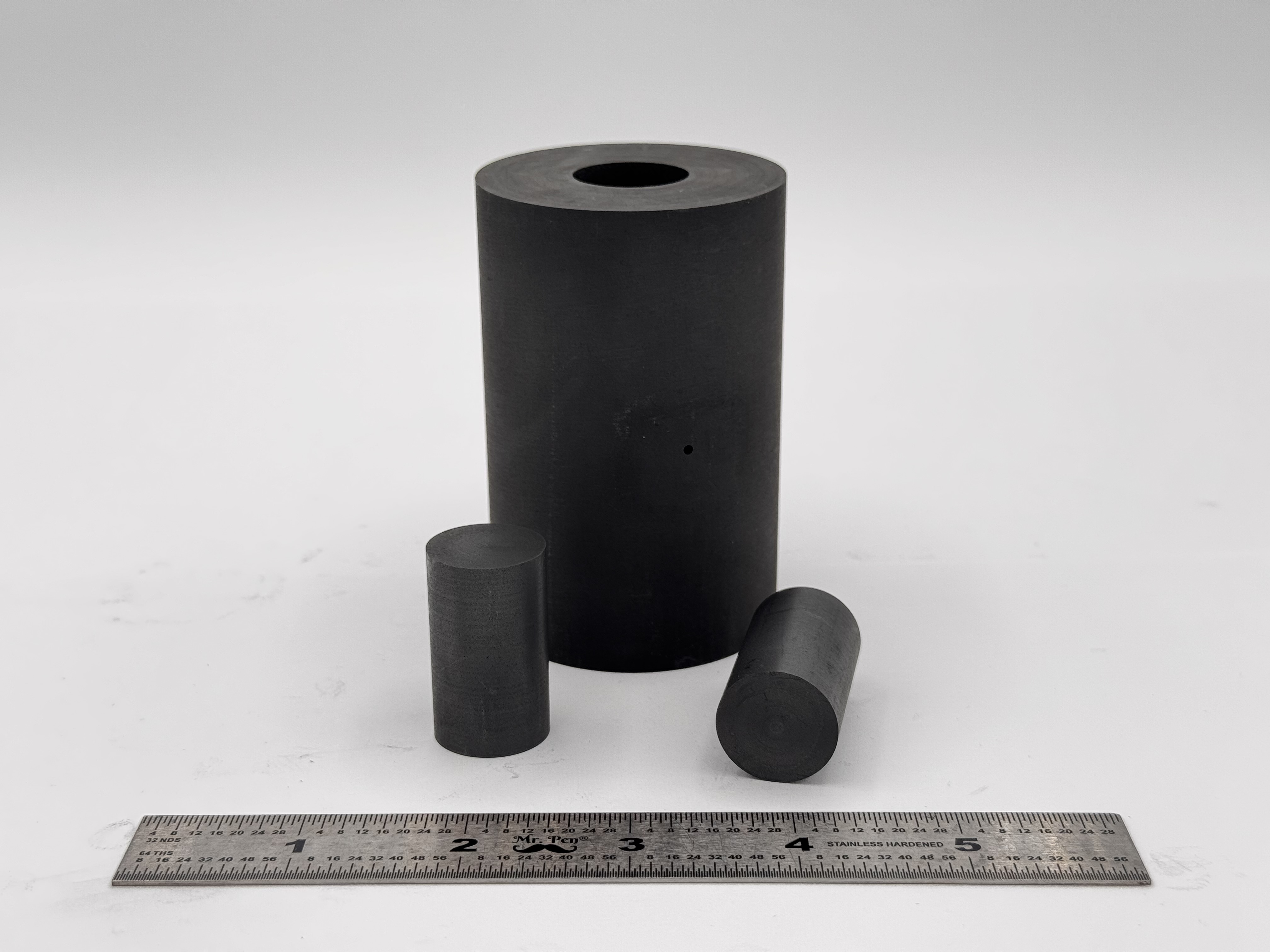
 High Strength SPS Graphite Tooling
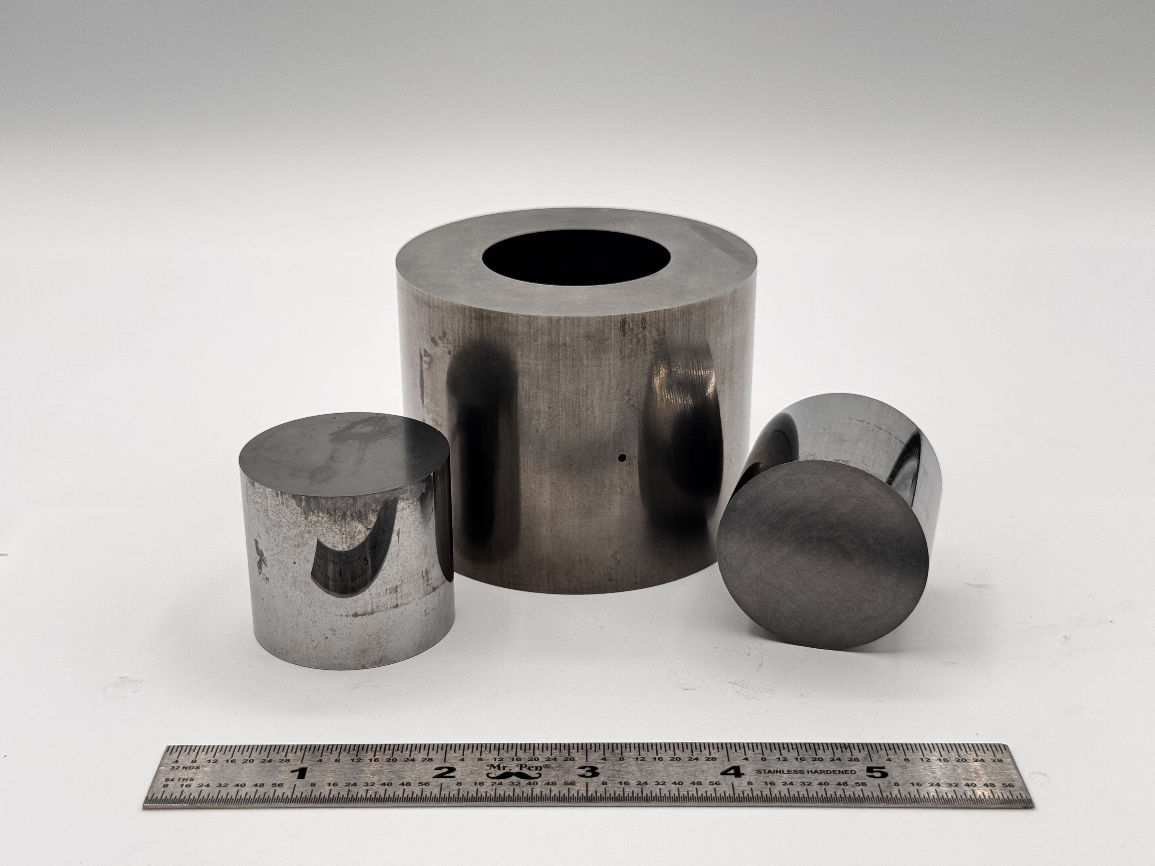 Tungsten Carbide Tooling
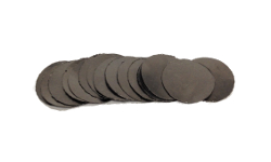 Carbon Graphite Foil / Paper
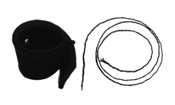 Carbon Felt and Yarn
 Spark Plasma Sintering Systems
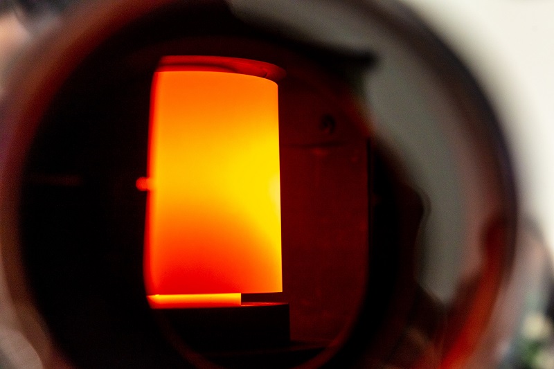 SPS/FAST Modeling Software
Tungsten Carbide Dies: The Unsung Enabler of Modern Nanotechnology Research
When people think about nanotechnology, they often imagine exotic materials, atom-scale engineering, and groundbreaking innovations in fields ranging from clean energy to aerospace. Rarely do they consider the tooling that makes many of these advancements possible. Yet behind countless breakthroughs in nanomaterials research stands a remarkably durable and often overlooked technology: the tungsten carbide die.
While tungsten carbide dies have long been associated with traditional manufacturing processes such as wire drawing, metal forming, and extrusion, their role has expanded significantly in recent decades. Today, they serve as critical enabling components in advanced powder metallurgy, nanoparticle production, cryomilling, and field-assisted sintering technologies. As nanotechnology continues to push materials science toward ever-smaller structures and increasingly complex material systems, tungsten carbide dies have become indispensable tools in both research laboratories and industrial production environments.
What Are Tungsten Carbide Dies?
Tungsten carbide dies are precision tooling components manufactured from a composite material consisting primarily of tungsten carbide (WC) particles bonded together with a metallic binder, typically cobalt. This combination creates a material that exhibits exceptional hardness, wear resistance, and compressive strength.
In fact, tungsten carbide is among the hardest engineering materials available, surpassed only by a handful of specialized ceramics and diamond. These properties allow carbide dies to withstand extreme pressures, repeated mechanical loading, and highly abrasive environments while maintaining dimensional accuracy over long operating lifetimes.
Traditionally, tungsten carbide dies have been used in applications such as:
- Wire drawing
- Tube drawing
- Metal extrusion
- Cold heading
- Stamping and forming
- Fastener manufacturing
However, as materials science has evolved, these same properties have made tungsten carbide an ideal choice for advanced nanotechnology applications.
The Challenge of Producing Nanomaterials
Nanotechnology often begins with powders. Whether researchers are developing advanced battery materials, high-entropy alloys, ceramic composites, magnetic materials, or nuclear materials, the ability to control particle size is critical.
The defining characteristic of nanomaterials is their extremely small grain or particle size, typically measured in billionths of a meter. Achieving these dimensions requires sophisticated processing methods capable of breaking down larger particles while maintaining strict control over contamination and material integrity.
This is where tungsten carbide first enters the nanotechnology workflow.
Tungsten Carbide in High-Energy Milling
One of the most common methods for producing nanopowders is high-energy mechanical milling. In these systems, powders are repeatedly fractured, cold welded, and refined through collisions with hardened milling media.
Tungsten carbide is widely used for:
- Milling jars
- Grinding media
- Attritor mill components
- Pulverizing equipment
- Mechanical alloying systems
Because tungsten carbide is significantly harder than conventional tool steels, it can efficiently reduce particle sizes into the nanometer range while resisting wear during prolonged processing cycles.
Researchers routinely rely on tungsten carbide tooling to produce:
- Nanocrystalline metals
- Ceramic nanopowders
- High-entropy alloy powders
- Magnetic materials
- Catalyst materials
- Battery electrode materials
Without wear-resistant milling systems, contamination levels would rise rapidly, compromising the quality and performance of advanced nanomaterials.
Cryomilling and the Production of Nanostructured Powders
The importance of tungsten carbide becomes even more pronounced during cryomilling.
Cryomilling is a specialized form of mechanical milling performed at extremely low temperatures, often using liquid nitrogen. These low temperatures suppress recovery and recrystallization mechanisms, allowing materials to develop ultrafine grain structures and nanocrystalline microstructures.
Cryomilling has become a valuable tool for producing:
- Nanocrystalline aluminum alloys
- Advanced titanium alloys
- Nanostructured steels
- High-entropy alloys
- Aerospace materials
- Defense-related materials
The intense impact forces generated during cryogenic processing place enormous demands on milling equipment. Tungsten carbide components provide the necessary durability to survive these conditions while maintaining dimensional stability and minimizing contamination.
For organizations focused on advanced powder production, cryomilling and tungsten carbide tooling often work hand in hand to create materials with properties that would be impossible to achieve through conventional manufacturing methods.
From Nanopowders to Functional Components
Producing nanopowders is only the first step.
To become useful engineering materials, powders must be consolidated into dense components while preserving the nanoscale structures that give them their unique properties.
This presents a significant challenge.
Traditional sintering methods often require long processing times and elevated temperatures, which can cause grain growth and eliminate the very nanostructures researchers worked so hard to create.
To address this challenge, advanced consolidation technologies such as Field-Assisted Sintering Technology (FAST) and Spark Plasma Sintering (SPS) have emerged as transformative manufacturing solutions.
The Critical Role of Tungsten Carbide Dies in FAST/SPS
FAST and SPS systems utilize pulsed direct electrical current and uniaxial pressure to rapidly consolidate powders into dense parts.
The process offers several advantages:
- Extremely rapid heating rates
- Reduced processing times
- Lower sintering temperatures
- Near-full densification
- Enhanced microstructural control
- Preservation of nanoscale grain structures
However, these benefits depend heavily on the tooling used during consolidation.
Tungsten carbide dies play a crucial role by:
- Containing powder during processing
- Applying high compressive forces
- Maintaining dimensional accuracy
- Resisting wear from repeated production cycles
- Supporting precision component manufacturing
In many advanced sintering systems, tungsten carbide tooling enables researchers to apply the pressures necessary to achieve full density while minimizing deformation and dimensional variation.
Without robust die materials, many of the advantages of FAST and SPS would be difficult to realize consistently.
Enabling High-Entropy Alloys and Advanced Materials
One of the fastest-growing areas of nanotechnology involves the development of high-entropy alloys (HEAs).
Unlike traditional alloys that rely on one primary element, HEAs contain multiple principal elements in near-equal proportions. These complex material systems can exhibit remarkable combinations of:
- Strength
- Hardness
- Corrosion resistance
- Thermal stability
- Radiation resistance
Researchers frequently use mechanical alloying, cryomilling, and FAST/SPS processing to produce HEAs with nanocrystalline microstructures.
Throughout this manufacturing chain, tungsten carbide tooling is often present at multiple stages:
- Mechanical alloying of powders
- Particle size refinement
- Cryogenic processing
- Powder consolidation
- Prototype component production
In this sense, tungsten carbide serves as a foundational technology that helps unlock the potential of next-generation materials.
Nanostructured Tungsten Carbide Itself
Interestingly, tungsten carbide is not only an enabling material—it is also becoming a subject of nanotechnology research.
Scientists have developed nanocrystalline tungsten carbide materials with grain sizes measured in nanometers rather than microns.
These materials often demonstrate:
- Increased hardness
- Improved wear resistance
- Enhanced mechanical properties
- Longer service life
- Better cutting performance
Applications include:
- Precision machining tools
- Semiconductor manufacturing equipment
- Wear-resistant industrial components
- Advanced tooling systems
The development of nano-grained tungsten carbide demonstrates how nanotechnology can improve even the materials that support nanotechnology itself.
Supporting Semiconductor and Microelectronics Manufacturing
Nanotechnology extends far beyond materials science.
The semiconductor industry routinely operates at dimensions measured in nanometers, requiring extraordinary precision throughout the manufacturing process.
Tungsten carbide tooling is frequently used in equipment that produces:
- Semiconductor wafers
- MEMS devices
- Advanced sensors
- Electronic packaging systems
- Microelectronic components
Its resistance to wear and deformation helps maintain the tight tolerances required for nanoscale manufacturing operations.
As semiconductor devices continue to shrink, the demand for precision tooling capable of maintaining microscopic accuracy becomes increasingly important.
Energy Technologies and Catalysis
Researchers are also exploring nano-sized tungsten carbide particles as functional materials in their own right.
Nanostructured tungsten carbide has demonstrated promising catalytic behavior in applications such as:
- Hydrogen production
- Fuel cells
- Electrocatalysis
- Chemical synthesis
- Energy conversion systems
In some reactions, nano-tungsten carbide exhibits catalytic characteristics similar to those of precious metals such as platinum, creating opportunities for lower-cost and more scalable energy technologies.
This emerging area of research highlights the growing influence of tungsten carbide not only as a processing tool but also as an advanced material platform.
A Hidden Foundation of Nanotechnology
Many of the most exciting developments in nanotechnology receive attention because of the remarkable properties they deliver. Stronger aerospace materials, more efficient batteries, advanced nuclear components, and next-generation electronics all capture headlines.
Yet the manufacturing infrastructure behind these innovations often remains invisible.
Tungsten carbide dies occupy a unique position within this ecosystem. They are rarely the final product, but they frequently make the final product possible.
From producing nanopowders through high-energy milling, to enabling cryomilling processes, to supporting advanced consolidation methods such as FAST and SPS, tungsten carbide dies help bridge the gap between scientific discovery and practical engineering solutions.
As nanotechnology continues to evolve, the demand for advanced powders, novel alloy systems, and highly controlled microstructures will only increase. Alongside these developments, tungsten carbide tooling will remain a critical enabler—quietly supporting the research, manufacturing, and innovation that drive the future of materials science.
In many ways, tungsten carbide dies are not simply tools used in nanotechnology. They are part of the foundational infrastructure that allows nanotechnology itself to exist.